Satish kashyap: microwind tutorial part 5 : three (3) input nand gate Nand nor gate transistor logic cmos why input circuit nmos gates size diagram preferred over level logical output industry capacitance Cmos nand gate circuit diagram
CMOS Logic Circuit Design for NOT, NAND and NOR Gate - YouTube
Nand input nor gates logic circuitlab Input nand gate three microwind stick diagram schematic tutorial part Circuit diagram of or gate using nand
Nand gate inputs logic resistor 74xx pull note need down
Integrated circuits logic gates pdfNand circuit gate diagram input draw Nand gate diagramMultisim input nand.
Digital logicNand-gate| digital logic gates || electronics tutorial Nand gate schematic diagramCmos nand gate circuit diagram.

Ttl nand explain truth transistors
How to draw the circuit diagram of 3 input nand gateNand cmos pmos nmos logic input transistors nor parallel transistor implementation logica turns switching which quasi delay insensitive gatter function Nand gate diagramE77 . lab 3 : laying out simple circuits.
Digital logic3 or 4 inputs nand gate Gate nand input electronics three logic digital tutorial gates figure above showsNand gate diagram.

74hc00 / 74hct00, quad 2
Nand circuitverseDigital logic nand gate(universal gate),its symbols & schematics [diagram] circuit diagram nand gateNand gate diagram.
In a 2-input nand, which will be faster when switching: when the aNand gate circuits integrated Draw the circuit diagram of ttl nand gate and explain its working withCmos nand gate circuit diagram.

Energy efficiency in schools: 3 input nand gate stick diagram
Nand gate schematic diagram3 input nand gate circuit diagram Cmos logic circuit design for not, nand and nor gateNand gate nmos logic schematic transistor digital using universal symbols its two given below.
[diagram] logic diagram using nand gateNand layout gate simple figure laying circuits larger version click Nand gate diagram 74hc00 ttl input quad 7400 pinout latch using gates nor push pull octoprint funny four has[diagram] circuit diagram nand gate.

[diagram] circuit diagram nand gate
Nand implementation transistorsNand gate circuit diagram ic 74ls00 pinout gates logic chip input circuitdigest circuits diagrams working electronic using explanation four limitations Nand gate layoutPin on elektronica.
.


Nand Gate Diagram
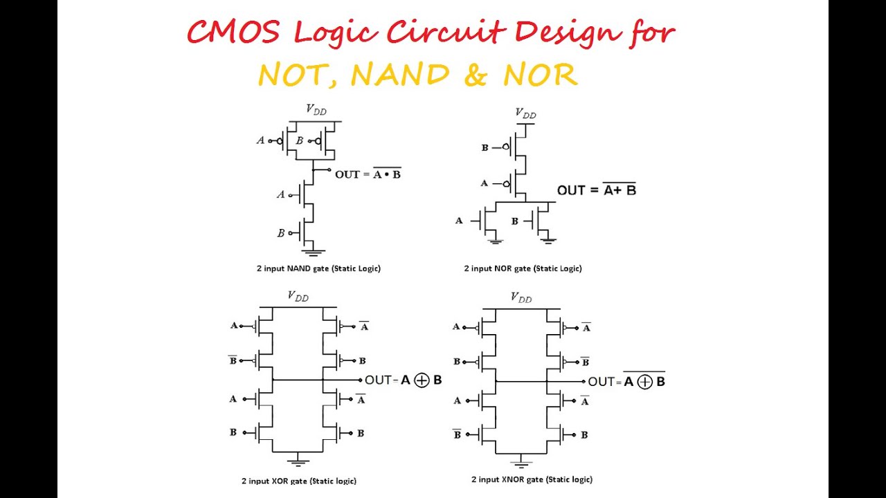
CMOS Logic Circuit Design for NOT, NAND and NOR Gate - YouTube

Pin on Elektronica
![[DIAGRAM] Circuit Diagram Nand Gate - MYDIAGRAM.ONLINE](https://i2.wp.com/cmosedu.com/jbaker/courses/ee421L/f13/students/wolvert9/Lab 6/2 input NAND gate schematic.JPG)
[DIAGRAM] Circuit Diagram Nand Gate - MYDIAGRAM.ONLINE

Cmos Nand Gate Circuit Diagram - Photos

Nand Gate Diagram

digital logic - Why is NAND gate preferred over NOR gate in industry